- 您现在的位置:买卖IC网 > Sheet目录3833 > PIC18F2455-I/SO (Microchip Technology)IC PIC MCU FLASH 12KX16 28SOIC
2009 Microchip Technology Inc.
DS39632E-page 113
PIC18F2455/2550/4455/4550
10.0 I/O PORTS
Depending on the device selected and features
enabled, there are up to five ports available. Some pins
of the I/O ports are multiplexed with an alternate
function from the peripheral features on the device. In
general, when a peripheral is enabled, that pin may not
be used as a general purpose I/O pin.
Each port has three registers for its operation. These
registers are:
TRIS register (data direction register)
PORT register (reads the levels on the pins of the
device)
LAT register (output latch)
The Data Latch register (LATA) is useful for read-
modify-write operations on the value driven by the I/O
pins.
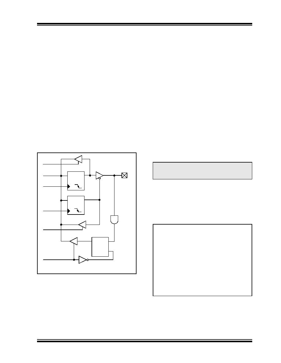
A simplified model of a generic I/O port, without the
interfaces to other peripherals, is shown in Figure 10-1.
FIGURE 10-1:
GENERIC I/O PORT
OPERATION
10.1
PORTA, TRISA and LATA Registers
PORTA is an 8-bit wide, bidirectional port. The corre-
sponding Data Direction register is TRISA. Setting a
TRISA bit (= 1) will make the corresponding PORTA pin
an input (i.e., put the corresponding output driver in a
high-impedance mode). Clearing a TRISA bit (= 0) will
make the corresponding PORTA pin an output (i.e., put
the contents of the output latch on the selected pin).
Reading the PORTA register reads the status of the
pins; writing to it will write to the port latch.
The Data Latch register (LATA) is also memory
mapped. Read-modify-write operations on the LATA
register read and write the latched output value for
PORTA.
The RA4 pin is multiplexed with the Timer0 module
clock input to become the RA4/T0CKI pin. The RA6 pin
is multiplexed with the main oscillator pin; it is enabled
as an oscillator or I/O pin by the selection of the main
oscillator
in
Configuration
Register
1H
(see
Section 25.1 “Configuration Bits” for details). When
not used as a port pin, RA6 and its associated TRIS
and LAT bits are read as ‘0’.
RA4 is also multiplexed with the USB module; it serves
as a receiver input from an external USB transceiver.
For details on configuration of the USB module, see
Several PORTA pins are multiplexed with analog inputs,
the analog VREF+ and VREF- inputs and the comparator
voltage reference output. The operation of pins RA5
and RA3:RA0 as A/D converter inputs is selected by
clearing/setting the control bits in the ADCON1 register
(A/D Control Register 1).
All other PORTA pins have TTL input levels and full
CMOS output drivers.
The TRISA register controls the direction of the RA
pins, even when they are being used as analog inputs.
The user must ensure the bits in the TRISA register are
maintained set when using them as analog inputs.
EXAMPLE 10-1:
INITIALIZING PORTA
Data
Bus
WR LAT
WR TRIS
RD PORT
Data Latch
TRIS Latch
RD TRIS
Input
Buffer
I/O pin(1)
Q
D
CK
Q
D
CK
EN
QD
EN
RD LAT
or PORT
Note 1:
I/O pins have diode protection to VDD and VSS.
Note:
On a Power-on Reset, RA5 and RA3:RA0
are configured as analog inputs and read
as ‘0’. RA4 is configured as a digital input.
CLRF
PORTA
; Initialize PORTA by
; clearing output
; data latches
CLRF
LATA
; Alternate method
; to clear output
; data latches
MOVLW
0Fh
; Configure A/D
MOVWF
ADCON1 ; for digital inputs
MOVLW
07h
; Configure comparators
MOVWF
CMCON
; for digital input
MOVLW
0CFh
; Value used to
; initialize data
; direction
MOVWF
TRISA
; Set RA<3:0> as inputs
; RA<5:4> as outputs
发布紧急采购,3分钟左右您将得到回复。
相关PDF资料
TS87C51RD2-VCL
IC MCU 8051 OTP 64K 5V 68PLCC
TS87C51RD2-MIL
IC MCU 8051 OTP 64K 5V 68PLCC
TS87C51RD2-MCM
IC MCU 8051 OTP 64K 5V 64VQFP
TS87C51RD2-MCL
IC MCU 8051 OTP 64K 5V 68PLCC
AT80C31X2-3CSUL
IC MCU 8031 ROMLESS 5V 40DIP
ATTINY11L-2SU
IC AVR MCU 1K FLASH 2MHZ 8SOIC
AT89S8253-24PC
IC 8051 MCU FLASH 12K 40DIP
AT89S8253-24JI
IC 8051 MCU FLASH 12K 44PLCC
相关代理商/技术参数
PIC18F2455-I/SO
制造商:Microchip Technology Inc 功能描述:IC 8BIT FLASH MCU 18F2455 SOIC28
PIC18F2455-I/SP
功能描述:8位微控制器 -MCU 24kBF 2048RM FSUSB2 RoHS:否 制造商:Silicon Labs 核心:8051 处理器系列:C8051F39x 数据总线宽度:8 bit 最大时钟频率:50 MHz 程序存储器大小:16 KB 数据 RAM 大小:1 KB 片上 ADC:Yes 工作电源电压:1.8 V to 3.6 V 工作温度范围:- 40 C to + 105 C 封装 / 箱体:QFN-20 安装风格:SMD/SMT
PIC18F2455-I/SP
制造商:Microchip Technology Inc 功能描述:8-Bit Microcontroller IC
PIC18F2455T-I/SO
功能描述:8位微控制器 -MCU 24kBF 2048RM FSUSB2 RoHS:否 制造商:Silicon Labs 核心:8051 处理器系列:C8051F39x 数据总线宽度:8 bit 最大时钟频率:50 MHz 程序存储器大小:16 KB 数据 RAM 大小:1 KB 片上 ADC:Yes 工作电源电压:1.8 V to 3.6 V 工作温度范围:- 40 C to + 105 C 封装 / 箱体:QFN-20 安装风格:SMD/SMT
PIC18F2458-I/SO
功能描述:8位微控制器 -MCU 24KB Flash 2KB RAM RoHS:否 制造商:Silicon Labs 核心:8051 处理器系列:C8051F39x 数据总线宽度:8 bit 最大时钟频率:50 MHz 程序存储器大小:16 KB 数据 RAM 大小:1 KB 片上 ADC:Yes 工作电源电压:1.8 V to 3.6 V 工作温度范围:- 40 C to + 105 C 封装 / 箱体:QFN-20 安装风格:SMD/SMT
PIC18F2458-I/SP
功能描述:8位微控制器 -MCU 24KB Flash 2KB RAM RoHS:否 制造商:Silicon Labs 核心:8051 处理器系列:C8051F39x 数据总线宽度:8 bit 最大时钟频率:50 MHz 程序存储器大小:16 KB 数据 RAM 大小:1 KB 片上 ADC:Yes 工作电源电压:1.8 V to 3.6 V 工作温度范围:- 40 C to + 105 C 封装 / 箱体:QFN-20 安装风格:SMD/SMT
PIC18F2458T-I/SO
功能描述:8位微控制器 -MCU 24KB Flash 2KB RAM RoHS:否 制造商:Silicon Labs 核心:8051 处理器系列:C8051F39x 数据总线宽度:8 bit 最大时钟频率:50 MHz 程序存储器大小:16 KB 数据 RAM 大小:1 KB 片上 ADC:Yes 工作电源电压:1.8 V to 3.6 V 工作温度范围:- 40 C to + 105 C 封装 / 箱体:QFN-20 安装风格:SMD/SMT
PIC18F2480-E/ML
功能描述:8位微控制器 -MCU 16 KB 768 RAM 25 I/O RoHS:否 制造商:Silicon Labs 核心:8051 处理器系列:C8051F39x 数据总线宽度:8 bit 最大时钟频率:50 MHz 程序存储器大小:16 KB 数据 RAM 大小:1 KB 片上 ADC:Yes 工作电源电压:1.8 V to 3.6 V 工作温度范围:- 40 C to + 105 C 封装 / 箱体:QFN-20 安装风格:SMD/SMT